Aurora Systems · SI/PI Design Automation (EDA)

Aurora Systems: Signal & Power Integrity Analysis Capabilities

Aurora Systems is GTECH ASIA's technology partner for signal and power integrity (SI/PI) design automation. This page works through what its verification and analysis workflow actually does for engineers building high-speed chip, package, and PCB interconnects, as a technical reference rather than a product pitch.

Platform ClassSI/PI design automation platform (EDA)
DeveloperAurora Systems (GTECH ASIA technology partner)
Core CapabilitiesLayout import, 3D EM extraction, SI/PI analysis, compliance checking, link simulation
Design ScaleDie-to-die chiplet interconnect through package and PCB-level assemblies
Typical DeploymentSemiconductor packaging, PCB, and IC design verification teams, pre-silicon sign-off
Overview

What Aurora Systems actually is

Aurora Systems supplies electronic design automation (EDA) software for signal and power integrity — a distinct discipline from the mechanical and structural CAE tools that make up most of GTECH ASIA's portfolio. Where Nastran or Marc predict how a physical structure deforms or heats up, Aurora's tools predict how an electrical signal or a power delivery network behaves as it moves through an IC package or printed circuit board: whether a data signal arrives clean enough to be read correctly at multi-gigabit-per-second rates, and whether a power rail supplies stable, low-noise voltage to the silicon that depends on it.

The specific product currently offered through GTECH ASIA is Aurora Appalachian, a die-to-die verification platform built around the UCIe (Universal Chiplet Interconnect Express) standard. As chip designs move away from single monolithic dies toward multi-die "chiplet" packages, the electrical interconnect between adjacent dies becomes its own verification problem — one with tight loss, crosstalk, and jitter budgets defined by the UCIe specification itself. Aurora Appalachian automates the flow from importing a package layout through electromagnetic extraction, compliance checking against the UCIe spec, system-level link simulation, and report generation, replacing what is otherwise a manual, multi-tool process spread across separate extraction, circuit-simulation, and documentation steps.

Because this is layout-driven, physics-based verification rather than schematic design, Aurora's tools sit downstream of package and PCB layout, consuming the same kind of geometric and stackup data that a mechanical or thermal simulation would consume — GDS and IRCX package files, layer stackups, and material properties — but solving Maxwell's equations and circuit-level transmission-line behavior instead of stress or heat transfer equations.

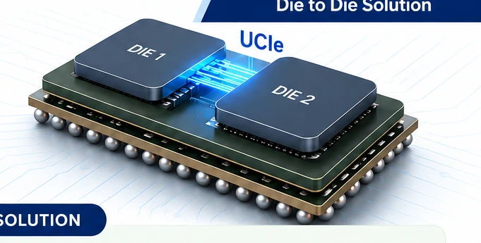
Two chiplet dies mounted on a BGA package substrate with a glowing UCIe die-to-die interconnect channel between them
A UCIe die-to-die interconnect between two chiplets on a shared package substrate — the physical interface Aurora Appalachian's verification flow is built around.
Capabilities

Seven core capabilities, explained

Each capability below is a distinct step in Aurora Appalachian's verification flow. For each one: what it solves, why engineers reach for it, the industries that depend on it most, the results it produces, and the design decisions those results are actually used to make.

01

Design Import & Interface Identification

Before any electrical analysis can run, the physical layout has to be read in and translated into a model the extraction engine understands. This means importing GDS (layout geometry) and IRCX (interconnect/stackup) files, resolving overlapping stackup definitions across a multi-die package, and — for a defined interface standard like UCIe — automatically detecting where the relevant signal groups actually are on the layout rather than requiring an engineer to hand-pick every trace and via. Automating interface identification matters because a modern chiplet package can carry hundreds of coupled signal lines, and manually locating and grouping every lane for a UCIe-A or UCIe-S interface is slow and error-prone at that scale.

Typical Industries
Semiconductor packaging, chiplet and advanced-package design, IC design verification teams.
Expected Outputs
A structured electrical model of the package or board, with signal groups and interfaces tagged for downstream extraction.
Design Decisions Enabled
Confirming the layout data and stackup are correctly represented before committing extraction and simulation time to them.
02

3D Electromagnetic Channel Extraction

Extraction is the step where physical geometry — trace width, spacing, via structure, dielectric stackup — becomes an electrical model: a set of S-parameters describing how the channel behaves across frequency. Aurora's extraction uses 3D electromagnetic field solving (HFSS-based) rather than simplified 2D approximations, and accounts for second-order effects that matter at multi-gigabit data rates: conductor surface roughness, through-silicon-via (TSV) parasitics, frequency-dependent material properties, and temperature-dependent conductivity. These effects are small individually but compound at high frequency, so a solver that ignores them will under-predict loss and give an overly optimistic read on channel performance.

Typical Industries
Semiconductor packaging, chiplet interconnect design, high-speed PCB design.
Expected Outputs
Frequency-dependent S-parameter models (channel behavior versus frequency) and port definitions for each extracted interface.
Design Decisions Enabled
Deciding whether a given trace geometry, via structure, or stackup needs to change before it goes further into the compliance and simulation flow.
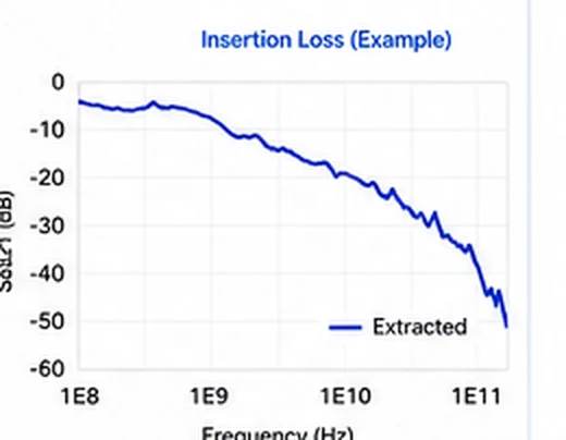
Insertion loss versus frequency chart, S21 in decibels plotted from 1E8 to 1E11 Hz
Insertion loss (S21) versus frequency — the standard measurement of how much signal energy a channel loses end-to-end.
03

Signal Integrity Analysis — Insertion Loss, Return Loss & Crosstalk

Signal integrity analysis characterizes how a high-speed electrical channel distorts the signals passing through it. Insertion loss measures how much signal energy is lost end-to-end at a given frequency; return loss measures how much signal reflects back toward the source because of impedance mismatches; crosstalk (near-end and far-end, NEXT/FEXT) measures how much energy couples from one signal line into its neighbors. Together these three measurements are the standard vocabulary engineers use to describe whether a channel is "clean" enough to carry a given data rate reliably, and they are computed directly from the extracted S-parameter model.

Typical Industries
Semiconductor packaging, high-speed PCB design, chip-to-chip and chiplet interconnect.
Expected Outputs
Insertion loss, return loss, and NEXT/FEXT crosstalk plotted against frequency for each signal path.
Design Decisions Enabled
Identifying which specific traces, vias, or coupling regions are driving loss or crosstalk so routing or spacing can be adjusted before layout is finalized.
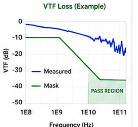
VTF loss versus frequency chart with a measured curve compared against a pass/fail mask, showing a pass region
A measured voltage transfer function (VTF) loss curve checked against the UCIe specification's mask — the channel stays inside the pass region at every plotted frequency.
04

High-Speed Interface Compliance Checking

Standards like UCIe define numeric limits a physical channel must meet — loss masks, crosstalk budgets, voltage transfer function (VTF) limits — at each supported data rate. Compliance checking takes the extracted and analyzed channel data and automatically compares it against the relevant standard's pass/fail mask, rather than requiring an engineer to manually cross-reference plotted results against a specification document. For UCIe specifically, this includes VTF loss and return loss mask validation and NEXT/FEXT crosstalk checks, evaluated per channel across the standard's defined data rates and versions.

Typical Industries
Semiconductor packaging, chiplet interconnect verification, any high-speed interface design governed by a published standard.
Expected Outputs
Automated pass/fail results per channel, with mask overlays showing margin (or violation) against the specification limit.
Design Decisions Enabled
Catching a non-compliant channel during the design phase, before it becomes a costly package or board re-spin discovered in silicon.
06

Power Integrity & Power Delivery Network Analysis

Power integrity is the counterpart discipline to signal integrity, and it's the "PI" half of Aurora Systems' SI/PI positioning. Where signal integrity is concerned with data signals, power integrity is concerned with the power delivery network (PDN) — the combination of package planes, PCB planes, vias, and decoupling capacitors that carries current from the board's voltage regulator to the die. As switching activity draws current in fast, uneven bursts, resistive and inductive parasitics in the PDN cause the delivered voltage to sag or ring (IR drop and voltage-rail noise), which can corrupt timing margins on the very signals signal integrity analysis is trying to protect. PDN analysis models this network's impedance versus frequency and its DC IR drop, and decoupling capacitor placement and value selection are tuned against that impedance profile to keep rail noise within the silicon's tolerance.

Typical Industries
Semiconductor packaging, IC and PCB power delivery design, high-current or high-switching-activity digital systems.
Expected Outputs
PDN impedance-versus-frequency curves, DC IR drop maps across the power plane, and decoupling network recommendations.
Design Decisions Enabled
Sizing and placing decoupling capacitors and power-plane structures so rail noise stays within the margin the digital and analog circuits actually need.
07

Automated Compliance Reporting

The final step in the flow converts extraction, compliance, and simulation results into a structured report — automated summaries covering design details, stackup information, loss and crosstalk results, compliance pass/fail status, and simulation outcomes, generated without manual slide-building. This matters less as a technical capability and more as a workflow one: SI/PI sign-off decisions typically need to be reviewed by people outside the extraction/simulation loop — program management, customers, or a design review board — and a consistent, automatically generated report format makes that review faster and more repeatable across projects.

Typical Industries
Semiconductor packaging programs, any design flow requiring formal SI/PI sign-off documentation.
Expected Outputs
Structured summary reports covering design, extraction, compliance, and simulation results with pass/fail status.
Design Decisions Enabled
Faster, more consistent sign-off review across engineering, management, and customer stakeholders.
Typical Workflow

How these capabilities connect in practice

An Aurora Appalachian verification run moves from layout import through extraction, analysis, compliance checking, and link simulation to a reviewable report.

Six-step workflow diagram: import design, block identification, channel extraction, compliance check, system simulation, report generation
The six-step verification flow Aurora Appalachian automates, from GDS/IRCX import through to an automated report.

Import the package or PCB layout

GDS and IRCX design files are read in, along with stackup and material definitions, and the relevant high-speed interfaces are identified and grouped.

Extract the electrical model

3D electromagnetic extraction converts the physical layout into frequency-dependent S-parameter models for each identified channel.

Run signal integrity or power integrity analysis

Insertion loss, return loss, and crosstalk are computed for signal channels; impedance and IR drop are computed for the power delivery network.

Check compliance against the interface specification

Results are compared automatically against the relevant standard's pass/fail mask (for example, UCIe's VTF loss and crosstalk limits) or against internal margin targets.

Simulate system-level link performance

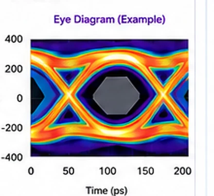
For channels of interest, extracted models are combined with driver/receiver behavioral models to generate eye diagrams and BER estimates.

Identify and fix violations, then re-verify

Where a channel fails compliance or shows poor eye margin, routing, via structure, stackup, or decoupling changes are made and the affected channels are re-extracted and re-checked.

Applications by Industry

Where these capabilities are put to work

Semiconductor & IC Packaging

The core application: die-to-die and chip-to-package interconnect verification for advanced packaging, including UCIe-based chiplet designs, where signal and power integrity issues caught late can force a costly package re-spin.

Consumer Electronics

High-speed digital interfaces inside compact consumer devices — where board space constraints tighten routing and increase crosstalk risk — benefit from the same insertion loss, crosstalk, and compliance checks applied at the PCB level.

Telecom & Networking

High-speed serial links in networking and telecom equipment operate at data rates where channel loss and jitter budgets are tight, making signal integrity and interface compliance verification a standard part of board and module design.

Automotive Electronics

As automotive electronics adopt higher-speed digital interfaces for sensor and compute connectivity, the same SI/PI verification discipline used in semiconductor and consumer design becomes relevant to automotive PCB and module design.

Interoperability

Where Aurora Systems fits in a wider design stack

Aurora Systems' SI/PI work is electronic design automation, which sits alongside — rather than tightly integrated with — the mechanical and structural CAE tools that make up the rest of GTECH ASIA's portfolio; the connection across the portfolio is mostly thematic rather than a shared solver or file format. Aurora's compliance and simulation results integrate directly with third-party circuit simulators ADS and HSPICE, and its extraction consumes IBIS/IBIS-AMI behavioral models, which are standard interchange formats in the SI/PI tool ecosystem rather than GTECH-specific integrations. Both Aurora Systems and the Cadence/MSC mechanical portfolio (Marc, Nastran) address electronics reliability from different angles — Aurora on electrical signal and power performance, Marc on the mechanical and thermal reliability of electronic assemblies — and GTECH ASIA positions the two as complementary parts of an overall electronics reliability capability rather than as a linked simulation chain. Where a design program needs both — for example, verifying that a package's thermal environment doesn't push material or interconnect behavior outside assumptions used in electrical extraction — that handoff today is a matter of shared design data and engineering judgment, not an automated data pipeline between Aurora and GTECH ASIA's mechanical CAE tools.

ADS & HSPICE

Third-party circuit simulators that consume Aurora's extracted channel models for system-level link simulation.

IBIS / IBIS-AMI Models

Standard behavioral models for driver and receiver circuits, used as the transmitter/receiver input to eye-diagram and BER simulation.

Addresses electronics reliability from the mechanical and thermal angle — a complementary discipline to Aurora's electrical signal and power verification, connected by shared design data rather than an automated pipeline.

Structural and thermal analysis of the same package or board assembly, part of the same broader electronics reliability picture GTECH ASIA positions alongside Aurora's SI/PI work.

FAQ

Frequently asked technical questions

What's the difference between signal integrity and power integrity analysis?

Signal integrity analysis looks at how data signals degrade as they travel through a channel — loss, reflection, and crosstalk affecting a specific signal path. Power integrity analysis looks at the power delivery network instead — how cleanly and stably voltage reaches the die from the board's regulator, accounting for IR drop and rail noise from switching current draw. The two are related because rail noise from a poorly designed power delivery network can corrupt the timing margin of signals that would otherwise pass signal integrity checks on their own.

Why does a UCIe interconnect need dedicated compliance checking rather than a general loss/crosstalk check?

Because UCIe defines specific numeric limits — voltage transfer function (VTF) loss masks, return loss limits, and crosstalk budgets — at each of its supported data rates and package types (UCIe-A and UCIe-S). A general "is loss low enough" check doesn't tell you whether a specific channel meets the specification's defined pass/fail mask at the data rate it's actually meant to run at; automated mask-based compliance checking does.

What's the difference between frequency-domain compliance checking and eye-diagram/BER simulation?

Frequency-domain compliance checking (loss, return loss, crosstalk masks) evaluates the channel itself in isolation. Eye-diagram and BER simulation adds the actual transmitter and receiver circuit behavior — via IBIS/IBIS-AMI models — on top of the extracted channel, predicting whether a real driver/receiver pair will actually close timing and voltage margin across that channel, which the channel-only view can't fully capture.

Why does channel extraction need to account for things like surface roughness and TSV effects instead of just trace geometry?

At multi-gigabit data rates, second-order effects that are negligible at lower frequencies — conductor surface roughness, through-silicon-via parasitics, frequency-dependent dielectric properties, temperature-dependent conductivity — become significant contributors to insertion loss. An extraction that ignores them will under-predict loss and produce an overly optimistic view of channel performance.

What design changes typically follow a failed compliance check?

Depending on which metric fails, the fix is usually one of: adjusting trace routing or spacing to reduce crosstalk, changing via structure or stackup to reduce loss or reflections, or modifying the decoupling network to reduce power-rail-induced signal degradation. The affected channel is then re-extracted and re-checked against the same compliance mask.

Does Aurora Systems replace circuit simulators like HSPICE, or work alongside them?

Alongside. Aurora's extraction and compliance checking generate the channel model and pass/fail results; system-level simulation integrates with ADS and HSPICE rather than replacing them, using the extracted model as the channel behind a circuit-level driver/receiver simulation.

GTECH ASIA supplies and supports Aurora Systems licensing for design verification teams across Malaysia and Southeast Asia, with HRD Corp certified training available for teams building in-house SI/PI verification capability.